


Electronics and enclosures ·
Release a sliding circuit board with a printed PCB ejector lever
A forked lever pivots on a separate metal pin at a prepared PCB edge. Its short nose bears against the enclosure to start the board moving out of its guides.
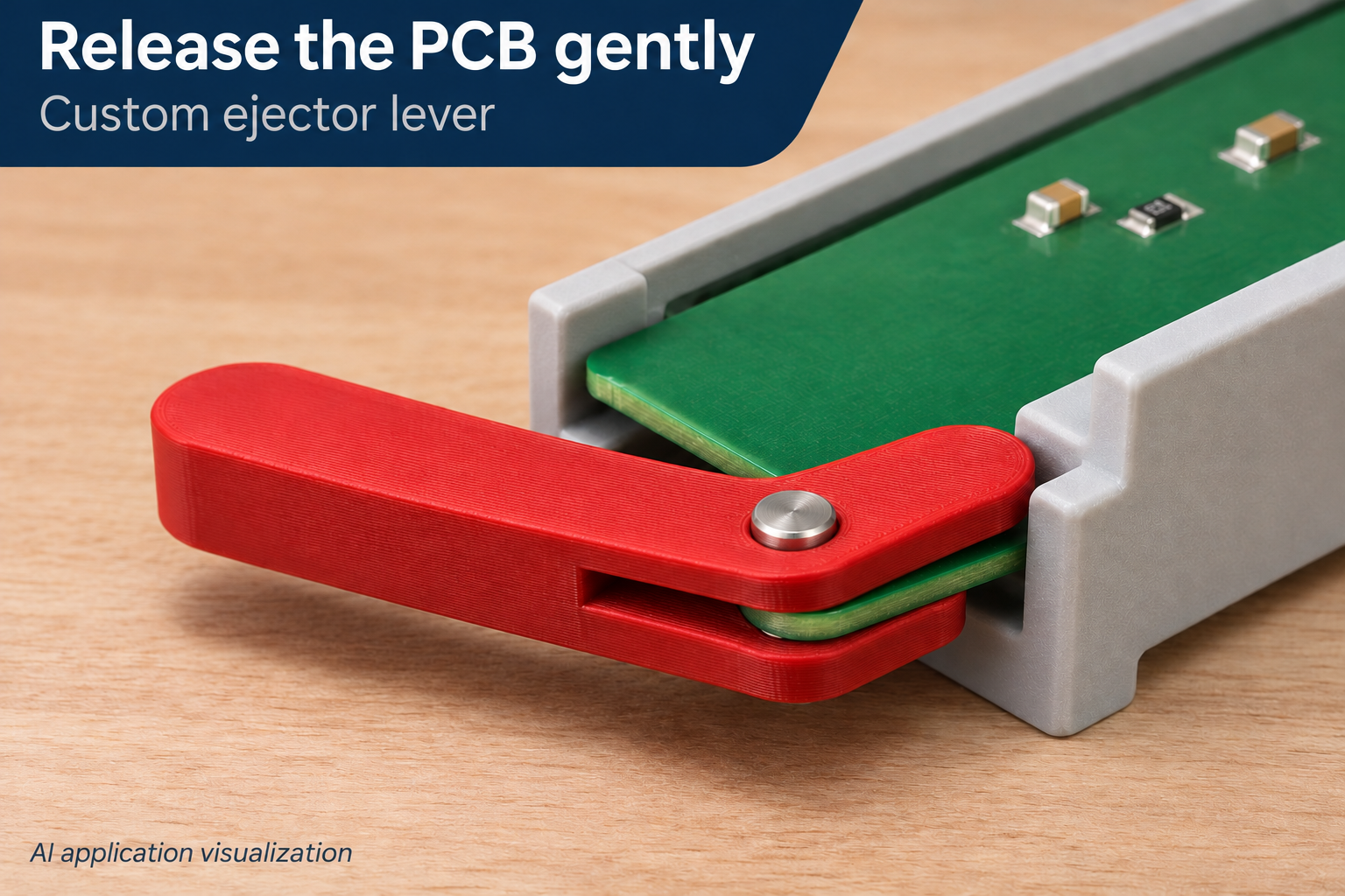
Give a small sliding board a release handle
A circuit board can be difficult to grip when its connector sits deep inside a hobby enclosure. This lever attaches to a prepared, component-free board edge. The PCB sits between two printed fork cheeks, and a separate metal pivot passes through both cheeks and a suitable existing mounting hole in the board.
The pivot travels with the PCB. The short lever nose bears against a fixed chassis stop. Swinging the long handle within the plane of the board can then start the withdrawal movement. Once released, the board is pulled along its guides.
Match the fork gap and pivot to the board
Board thickness is adjustable from 1 to 3.2 mm, with an additional total clearance of 0.2–0.8 mm. The initial values of 1.6 and 0.4 mm produce a 2 mm fork gap. This clearance applies to the whole gap, not separately to each face. Allow for burrs and the actual printed surface too.
Each cheek can be 2–4 mm thick, and the pivot hole can be 2.2–4.4 mm in diameter. Choose a suitable metal pin and retention arrangement that lets the lever rotate without crushing the PCB. Avoid using a coarse threaded section as the bearing surface at the pivot.
Design the reaction stop and movement together
The handle-length parameter ranges from 22 to 55 mm, initially 35 mm. Lever width is 6–12 mm and nose projection is 4–12 mm. These settings do not establish compatibility with an existing chassis. The nose, reaction stop and guides must be positioned so the initial movement withdraws the board without skewing or jamming it.
Test a first print on a disconnected, unpowered low-voltage hobby assembly. Use a deliberately provided hole in a clear PCB area rather than drilling through traces. Leave room for the handle to swing and check that the nose remains engaged with the reaction stop. Do not lever against components or force a stuck connector. The pin, board and chassis stop are separate items; no rated extraction force or physically verified load capacity is supplied.
The image is an AI application visualization, not a photograph of a physically tested print. Illustrated accessories are not included in the STL.
Next step